- 您现在的位置:买卖IC网 > Sheet目录1889 > AD5174BRMZ-10-RL7 (Analog Devices Inc)IC DGTL POT 1024POS 10K 10MSOP
AD5174
Rev. B | Page 7 of 20
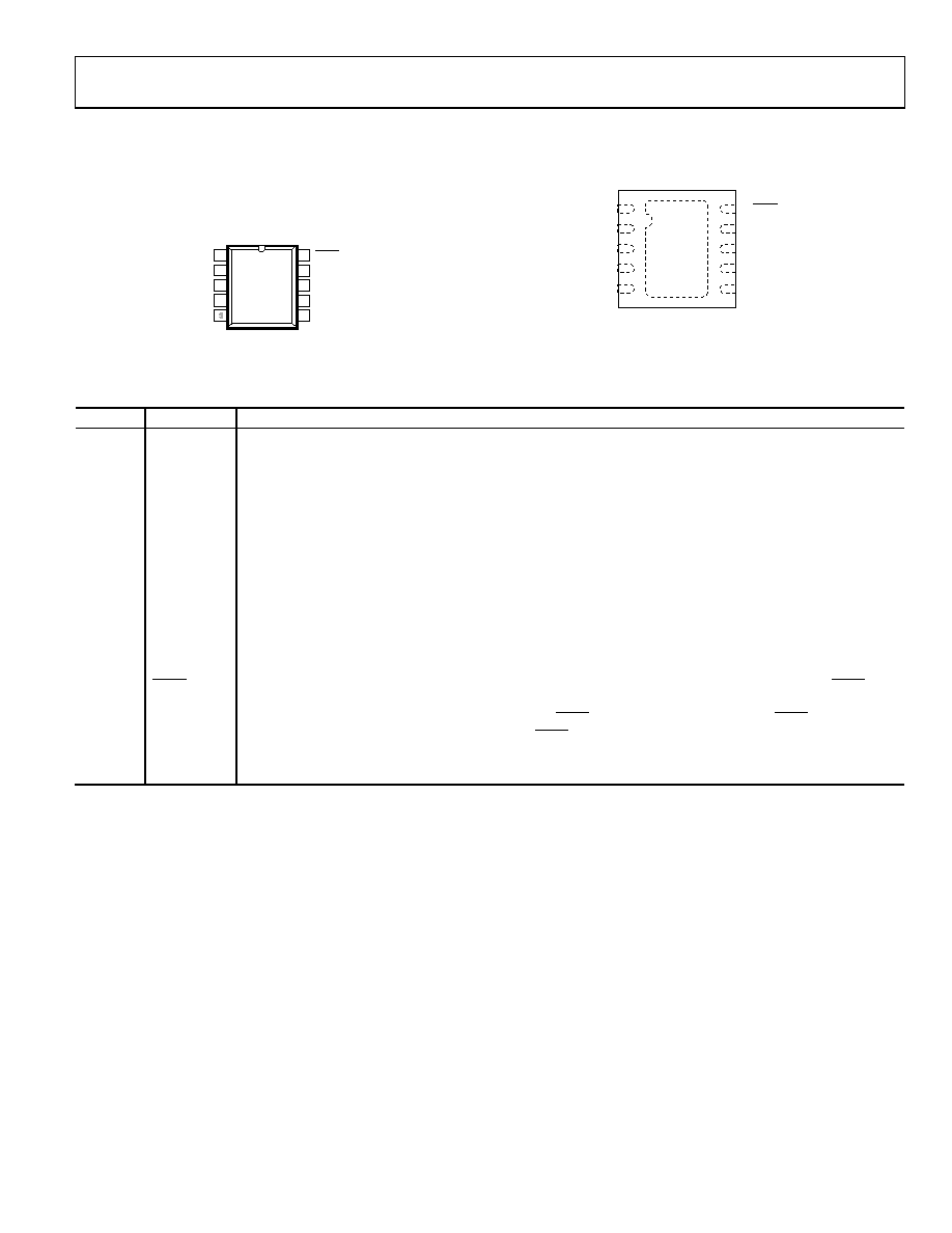
PIN CONFIGURATION AND FUNCTION DESCRIPTIONS
VDD 11
VSS
2
A
3
W
4
SDO
10
9
8
SCLK
7
5
EXT_CAP
DIN
6
GND
AD5174
TOP VIEW
(Not to Scale)
SYNC
08
718
-00
5
SYNC
VDD 1
VSS
2
A
3
W
4
SDO
10
9
8
SCLK
7
5
EXT_CAP
DIN
6 GND
*LEAVE FLOATING OR CONNECTED TO VSS.
AD5174
(EXPOSED
PAD)*
08
71
8-
1
0
3
Figure 5. MSOP Pin Configuration
Figure 6. LFCSP Pin Configuration
Table 5. Pin Function Descriptions
Pin No.
Mnemonic
Description
1
VDD
Positive Power Supply. Decouple this pin with 0.1 μF ceramic capacitors and 10 μF capacitors.
2
A
Terminal A of RDAC. VSS ≤ VA ≤ VDD.
3
W
Wiper Terminal of RDAC. VSS ≤ VW ≤ VDD.
4
VSS
Negative Supply. Connect to 0 V for single-supply applications. Decouple this pin with 0.1 μF ceramic capacitors
and 10 μF capacitors.
5
EXT_CAP
External Capacitor. Connect a 1 μF capacitor between EXT_CAP and VSS. This capacitor must have a voltage
rating of ≥7 V.
6
GND
Ground Pin, Logic Ground Reference.
7
SDO
Serial Data Output. This pin can be used to clock data from the shift register in daisy-chain mode or in readback
mode. This open-drain output requires an external pull-up resistor even if it is not use.
8
DIN
Serial Data Line. This pin is used in conjunction with the SCLK line to clock data into or out of the 16-bit
input register.
9
SCLK
Serial Clock Input. Data is clocked into the shift register on the falling edge of the serial clock input. Data can be
transferred at rates of up to 50 MHz.
10
SYNC
Falling Edge Synchronization Signal. This is the frame synchronization signal for the input data. When SYNC
goes low, it enables the shift register and data is transferred in on the falling edges of the subsequent clocks.
The selected register is updated on the rising edge of SYNC following the 16th clock cycle. If SYNC is taken
high before the 16th clock cycle, the rising edge of SYNC acts as an interrupt, and the write sequence is ignored
by the RDAC.
EPAD
Exposed Pad
Leave floating or connected to VSS
发布紧急采购,3分钟左右您将得到回复。
相关PDF资料
AD5175BRMZ-10-RL7
IC DGTL POT 1024POS 10K 10MSOP
AD5200BRMZ50-REEL7
IC POT DGTL 50K 256POS 10MSOP
AD5203ARZ100
IC POT DGTL QUAD 64POS 24SOIC
AD5204BRZ50
IC DGTL POT QUAD 50K 24-SOIC
AD5207BRU50
IC DGTL POT DUAL 256POS 14TSSOP
AD5220BNZ50
IC POT DGTL SGL 128POS 8DIP
AD5222BRUZ100
IC POT DGTL DUAL 128POS 14TSSOP
AD5227BUJZ10-R2
IC DGTL POT 10K UP/DN TSOT23-8
相关代理商/技术参数
AD5175
制造商:AD 制造商全称:Analog Devices 功能描述:Single-Channel, 1024-Position, Digital Rheostat with I2C Interface and 50-TP Memory
AD5175BCPZ-10-R2
制造商:AD 制造商全称:Analog Devices 功能描述:Single-Channel, 1024-Position, Digital Rheostat with I2C Interface and 50-TP Memory
AD5175BCPZ-10-RL7
功能描述:IC RHEOSTAT 5V 50-TP 1024 10MSOP RoHS:是 类别:集成电路 (IC) >> 数据采集 - 数字电位器 系列:- 标准包装:3,000 系列:DPP 接片:32 电阻(欧姆):10k 电路数:1 温度系数:标准值 300 ppm/°C 存储器类型:非易失 接口:3 线串行(芯片选择,递增,增/减) 电源电压:2.5 V ~ 6 V 工作温度:-40°C ~ 85°C 安装类型:表面贴装 封装/外壳:8-WFDFN 裸露焊盘 供应商设备封装:8-TDFN(2x3) 包装:带卷 (TR)
AD5175BRMZ-10
功能描述:IC DGTL POT 1024POS 10K 10MSOP RoHS:是 类别:集成电路 (IC) >> 数据采集 - 数字电位器 系列:- 标准包装:3,300 系列:WiperLock™ 接片:257 电阻(欧姆):100k 电路数:1 温度系数:标准值 150 ppm/°C 存储器类型:易失 接口:3 线 SPI(芯片选择) 电源电压:1.8 V ~ 5.5 V 工作温度:-40°C ~ 125°C 安装类型:表面贴装 封装/外壳:8-VDFN 裸露焊盘 供应商设备封装:8-DFN-EP(3x3) 包装:带卷 (TR)
AD5175BRMZ-10-RL7
功能描述:IC DGTL POT 1024POS 10K 10MSOP RoHS:是 类别:集成电路 (IC) >> 数据采集 - 数字电位器 系列:- 标准包装:3,000 系列:DPP 接片:32 电阻(欧姆):10k 电路数:1 温度系数:标准值 300 ppm/°C 存储器类型:非易失 接口:3 线串行(芯片选择,递增,增/减) 电源电压:2.5 V ~ 6 V 工作温度:-40°C ~ 85°C 安装类型:表面贴装 封装/外壳:8-WFDFN 裸露焊盘 供应商设备封装:8-TDFN(2x3) 包装:带卷 (TR)
AD5175JH
制造商:Analog Devices 功能描述:5175JH
AD517J
制造商:AD 制造商全称:Analog Devices 功能描述:Low Cost, Laser Trimmed, Precision IC Op Amp
AD517JH
制造商:Rochester Electronics LLC 功能描述:LOW IB, IOS, VOS OP AMP - Bulk